

The lectures during my last semester were largely focused on digital image processing. Combining this with the inspiration for 3D printing, I gathered through my trip though South Korea, resulted in the following seminar paper. Seminars are a compulsory part of our curriculum which I like due the self-contained work and the ability to pick an individual topic.
Over the past year, I’ve built my own Kossel 3D printer. The Mini Kossel is based on a novel parallel delta kinematic which was developed by Johann C. Rocholl, a Google engineer from Germany.
This paper is targeting the automation of solder paste dispensing onto printed circuit boards by using computer vision and RepRap robots.
Full Slides as PDF
Full Paper as PDF
Source Code at GitHub
Seminar: Image Processing and Content Analysis
Camera-based PCB Analysis for Solder Paste Dispensing
Steffen Vogel (steffen.vogel@rwth-aachen.de)
Academic Advisor: Wei Li (wei.li@lfb.rwth-aachen.de)
Institute of Imaging & Computer Vision (LfB)
Rheinisch-Westfälische Technische Hochschule (RWTH), 52056 Aachen
1 Abstract
Two of the main challenges for PCB prototyping are the time-consuming setup of involved machines and their economic feasibility for small laboratories and hobbyists. This paper tries to offer solutions for both of these issues:
- The complex setup process of industrial machines can be accelerated by computer vision. It is preferable to automate this process as far as possible to enable the operation by untrained personnel and hobbyists. The workflow can be further simplified by not relying on external CAD data. This includes: detection of components, pads and footprints; mapping between available components and footprints and planning of shortest tool paths.
- The adaption of proven 3D printers allows to lower the costs for such machines. The lightweight and fast kinematics of parallel 3D-delta robots like the RepRap Mini Kossel are perfectly suited for the assembly of PCBs. Only the print head has to be exchanged between the individual steps of the process.
This work presents a workflow to control DIY 3D printers for the purpose of PCB assembly. By using cheap and easy-obtainable parts like proven RepRap 3D printers, this technique is viable for small laboratories, FabLabs and hobbyists. During the seminar, a analysis and control software for RepRap printers was written. Hence, we focus on the overall workflow and tools and less on algorithms and theory.
Here, the task of solder paste dispensing was chosen to be explored in detail. This work establishes the groundwork for more complex task like the pick and placing of electronic components.
2 Motivation
The ongoing miniaturization of electronic products like smartphones and Ultra Books has led to a new form factor for electronic components. Surface-mounted devices (SMD) are already widespread in electronic design and production. As a result, previously used through-hole components are gradually phased out. This miniaturization of SMD components is an ongoing trend and raises the barrier for hobbyists to produce PCBs themselves. Soldering and placement of 0401-sized resistors or BGA packages is not possible by hand any longer.
This work is motivated by the vision to build an all-in-one machine for the complete process of prototype PCB assembly (PCBA). To accelerate the development process and to reduce the costs, all of these tasks can be handled by a single workbench 3D printer / CNC mill. The PCB production process roughly can consists of the following steps:
- Isolation milling or pen plotting of PCB traces
- Drilling of holes and contours
- Solder paste dispensing for SMD pads with a syringe
- Pick-and-place of SMT components with vacuum
- Soldering with hot air, a hot plate or by a laser
For the scope of this paper, the process of solder paste dispensing was chosen. This task offers the biggest margin to profit from computer vision. Industrial mass production uses stencils to apply solder paste onto the PCB. For small prototype assemblies the fabrication of stencils is not worthwhile. Therefore, solder paste is applied manually with a pressurized syringe, which is hold by hand.
The dispensing of solder paste requires the knowledge exact solder pad positions and dimensions. Traditionally, this information is exported by CAD design tools and is required to produce the stencils.
But sometimes the CAD data is not available or stored in an inaccessible proprietary format. This paper presents techniques to gather the pad locations and dimensions by means of computer vision.


3 Workflow
The task of solder paste dispensing can be further separated in several sub stages, which are explained in the following sections.
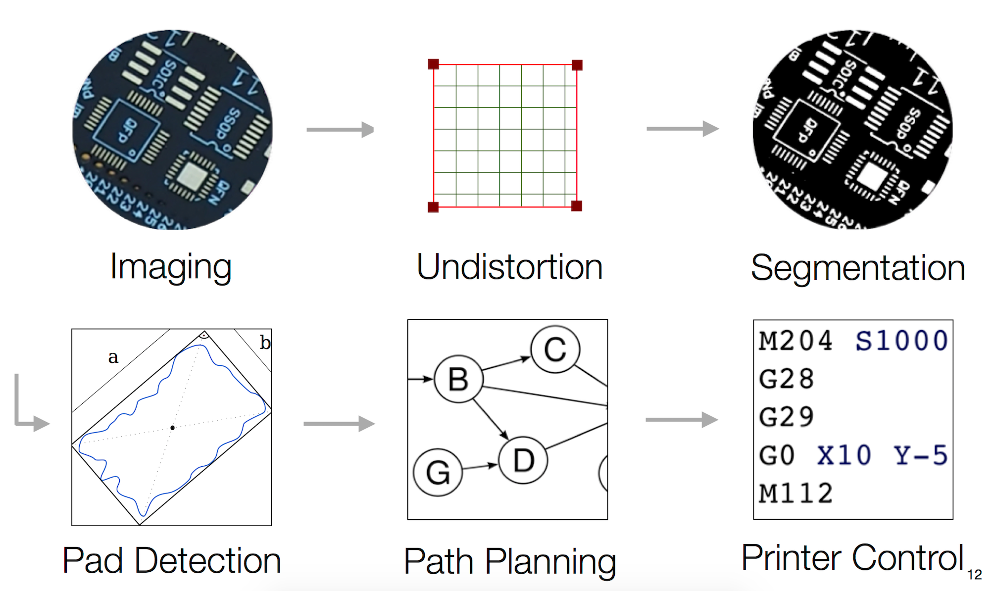
3.1 Imaging
In the original proposal, a webcam was planed be used to capture images for further analysis. But using other image sources like scanners or digital cameras has proven to provide superior image quality (see Table 1).
The resolution of a webcam is insufficient to capture the complete PCB in a single image. Even with a high resolution webcam1 satisfying results were only achievable by stitching several detailed shots together.
This issue can easily be resolved by using a professional digital camera (see Figure 3d). However, this prevents the direct attachment of the camera to the print head of the printer, because the weight of a camera would increase the inertance and thereby limit the maximum speed of the printer. The workflow does not require the image acquisition to be done on top of the working area of the printer.
By using cameras, all images are subject to distortion caused by lenses and perspective projection. This issue can be solved by calibrating the camera and by applying the inverse perspective transformation. These disadvantages can be avoided by using an imaging method which does not impose these distortions like a flatbed scanner. First tests showed biased results (see Figure 3c and 3a).
The previous methods do not rely on the existence of CAD layout data. In the end, best results can be achieved by directly using available CAD data (see Figure 3b). The industry uses a widespread format called Gerber for exchanging PCB layouts used for production. Almost every CAD tool can export PCB layouts as a Gerber file.
This Gerber format stores every part of the design (silkscreen, pads, board contour, milling, coper) in a separate layer. Basically it is a vector graphic format, whose layers are built out of basic geometric shapes. This allows them to be rendered to raster images of arbitrary resolutions2.


3.2 Undistortion
Camera-based imaging methods are subject to distortions caused by optical lenses. These non-linear distortions must be compensated by camera calibration.
During the camera calibration, a set of distortion parameters and a camera matrix is determined. Usually, a set of different views of a known pattern is used to measure the distortion coefficients. In this seminar, both chessboard and circle patterns were used. But it has become apparent, that non-linear distortions are mostly negligible when using recent DSLRs because most of them already compensate them by their internal image processing pipeline.
The workflow involves several different coordinate systems (C, U, R, S, P). This stage transforms the source image from the camera coordinate system C to the system of undistorted images U.

3.3 Perspective Correction
Camera-based imaging methods are also subject to perspective projection. The following analysis demands a top view onto the PCB. Thus, the perspective projection is turned into a two-dimensional euclidean plane.
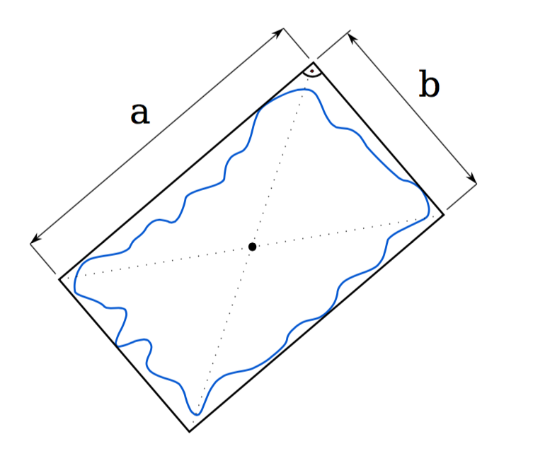
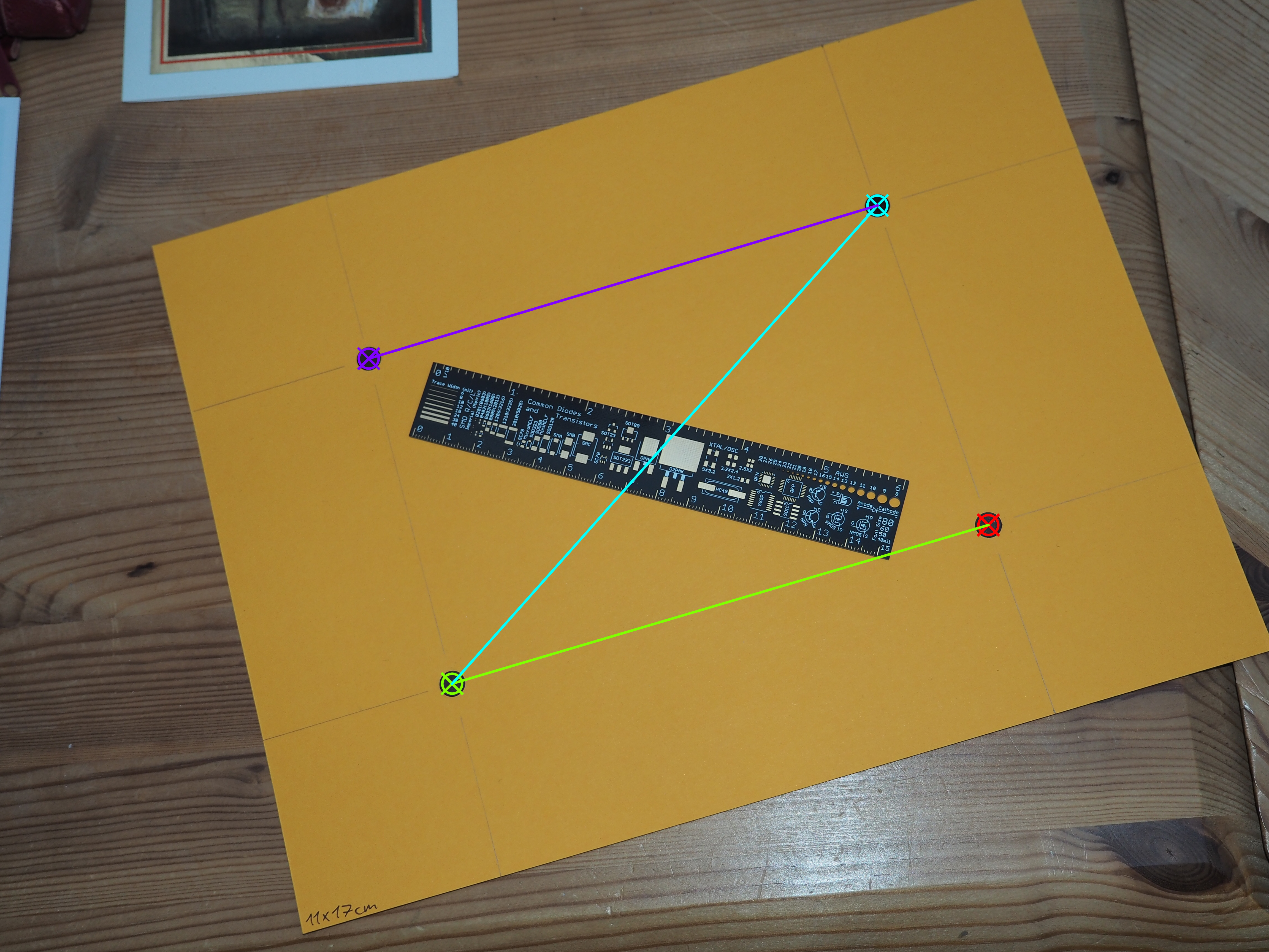
To simplify the correction, we assume that the PCB has a rectangular shape with known dimensions (w × h). This can be realized by enclosing the PCB with a set of four markers which are arranged in a rectangle as shown in Figure 9a.
The camera projection warps this rectangle into a quadrilateral shape. Mathematically, this is described by a perspective transformation between two coordinate systems. The undistorted image with coordinate system U has to be mapped to the reference system R.
The required transformation matrix is obtained by solving equation 1 with four points x of the image plane and their matching counterparts x′ of the object plane. The points of the object plane are given by the known dimensions and spacings of the markers or PCB3. In other words, respective markers are used to describe basis vectors for the reference coordinate system. Figure 9a shows the original image with the detected markers. Figure 9b shows the same image after the correction. Note that the markers are still partially visible in the corners of the warped image.

3.4 Preprocessing
The previous steps are mandatory for camera based imaging methods. Scans or CAD imported Gerber files already provide a top view onto the PCB, and therefore, allow skipping the previous stages.
Before starting with the segmentation of PCB solder joints, several preprocessing steps have to be executed. They improve the results of the following steps or allow saving computational time.
- Blurring: The segmentation relies on clustering and thresholding to detect solder joints. A prior smoothing of the image helps to cope with noise in the source image.
- Scaling: To reduce the required computational time, the source image is restricted to a sufficient resolution. In rare cases the resolution of the source image is too low for further analysis. In this case, the image is scaled up. This way the following algorithms can work with sub-pixel accuracy.
- Alignment: Subsequent steps are using morphological image operations to improve the results. These operations are using square-shaped kernels. By aligning the orientation of the PCB and its pads to the shape of the kernel, details and sharp edges of PCB pads are preserved. Furthermore, certain algorithms like the Harris edge detector can profit from known orientations of the vertices. The alignment can be identified by evaluation of Hough lines or the polar magnitude spectrum of and FFT (see [BreierLfB]).
3.5 Segmentation
To separate the solder pads from the remaining PCB and the background, a color-based segmentation method is used.
The K-Means clustering algorithm reduces the color space to k clusters. Usually, these classes correspondent to four portions of the PCB. These portions are ordered according to their occurrences in the image.
- Image background
- PCB base material (solder mask)
- Solder pads
- Silkscreen4
Hence, it makes sense to use k = 4 for the algorithm. Figure 10a shows the result of the K-Means algorithm. The correct selection of the solder pad class is crucial for valid results. Therefore, it is advisable to make use of more criteria for its selection. The current implementation only consults the frequency of each class. Additionally, the amount of connected objects per class might be used. The background and base material classes often only consist of a few connected objects. The solder pad class in contrast often has hundreds of individual objects.
Once a class has been selected (potentially by hand), a binary image is created. The resulting binary image is shown in Figure 10b.
3.6 Pad Detection & Filtering
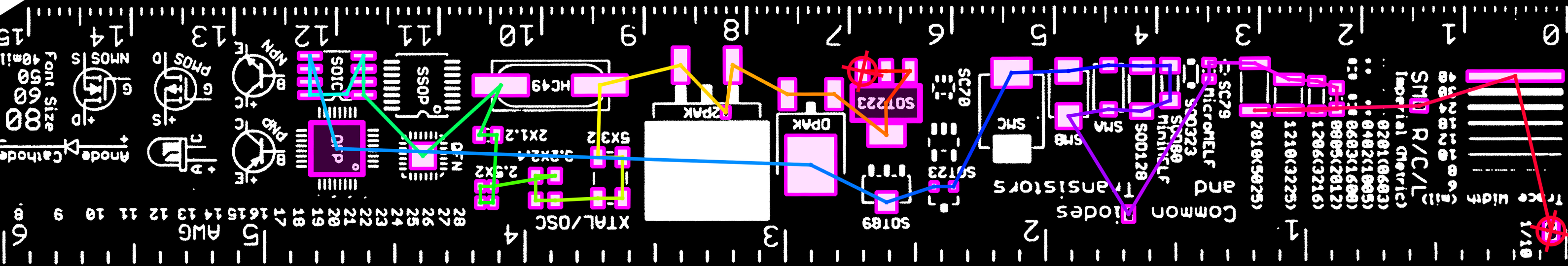
For solder paste dispensing, solder pad coordinates must be exactly located onto the PCB. In this paper, the detection is limited to pads with a rectangular shape as shown in Figure 2b. This limitation is negligible for most SMD packages, as they generally are using rectangular pads like shown in Figure 4.
The previous segmentation step produces in a binary image. This image is used to find contours, which are then used to analyse the shape of the invidual objects. These contours are filtered and classified by the following criteria:


In a first attempt, polygons were used to approximate the contour. The Ramer-Douglas-Peucker algorithm finds a polygon with as little as possible vertices. At the same time, the maximum deviation to the original contour is limited by a threshold. To qualify the contour as a solder pad, the approximated polygon must be a quadrangle, convex and the angles must be close to 90 degrees. This approach only delivered unsatisfying results because of the low resolution and random starting points of the contours, which do not coincide with the corners of the rectangle.
Better results can be achieved by comparing the enclosed area of a contour with the area of its minimal bounding rectangle (see Figure 5). A ratio above 0.8 usually yields a usable hit rate. Figure 10c shows the found rectangles (magenta frames).

Subsequently, the rectangles are filtered by their absolute area and aspect ratio. Overlapping rectangles are not allowed and are filtered out as well. Figure 10d shows the pads after these plausibility checks.
3.7 Tool Path Planning
To speed-up the execution, the pads have to be arrange in an order which results in a path with the minimum length. To find an optimal tool path, a hamiltonian path with minimum length must be determined. A hamiltonian path connects all vertices of a graph. We can think of the set of detected pads as a fully connected graph. Each edge is
weighted by the euclidean distance between the connected edges.
This problem description is a little different to other well known problems:
- Traveling Salesman Problem: The TSP looks for the shortest hamiltonian cycle (equal start end end nodes). For apply the solder paste, this constraint is dispensable. Apart from that, the TSP describes the problem quiet well. Most TSP solvers are designed for huge problem sizes (> 1000). This does not fit to our problem where usually 100-400 pads must be visited.
- Shortest Path Problem: There is a large amount of algorithms which find the shortest path between two vertices of a graph. This problem usually is faced for navigation. The Dijkstra algorithm is a well known representative in this category. The shortest path problem only describes the shortest path between two vertices of a graph and is therefore not suitable for the described case.
For this task, a simple nearest neighbor heuristic (NNR) was implemented. This heuristic starts with a random vertex and successively travels along the edge with the lowest weight, which corresponds to the nearest neighbor. However, this procedure will not result in an optimal path. The results can be easily improved by repeating the heuristic with different start vertices. Finally, the one which results in the minimal length is selected. This is known as the repetitive nearest neighbor (RNNR). Figure 10e shows the final result with the found path as an overlay.
3.8 Robot Control
Equation 1 shows the transformation between the undistorted camera images and reference coordinates. Similarly, another transformation between the reference system and the robot coordinate system is necessary.
Both the reference system R and the printer system P are two dimensional euclidean planes. We can map points (pads) from the reference system by scaling, rotating and translating them. Mathematically, this can be modeled by an affine transformation5:
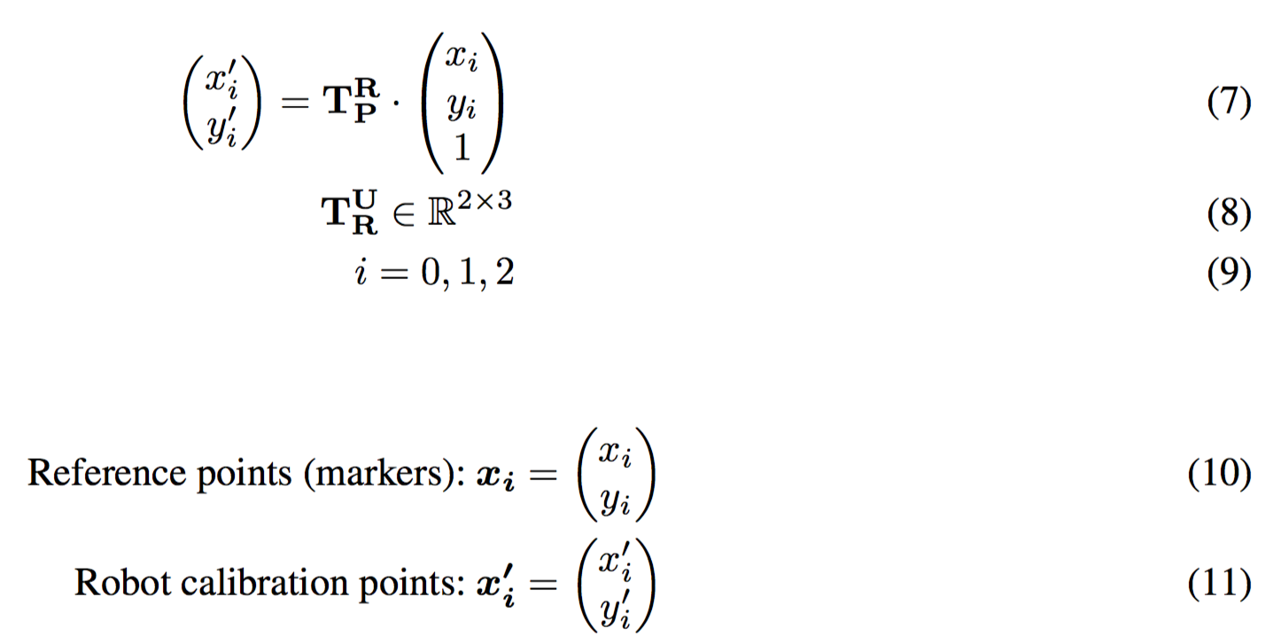
The coordinates of the reference markers xi are given by the corners of the processed image. The robot calibration points x′i have to be determined manually by aligning the printhead with markers of on the PCB, which is positioned on its working area. Once the print head is positioned over the marker (or corner of the PCB), the related printer coordinates are requested from the printer controller.
4 System Description
This section shortly describes the overall system design and used hardware. The system consists of a modified 3D printer which is capable to extrude solder paste6 and a common digital camera. Additionally, a laptop, PC or embedded system is used to carry out the computation.
4.1 Camera: Olympus OM-D E-M10
As shown in Table 1, digital cameras offer the best image quality and flexibility. Good lighting is crucial for satisfactory results. Shadows, uneven exposure and reflexions are the main issues during the analysis. The results in this paper we produced with a dedicated flash to provide indirect and diffuse illumination.
For enhanced usability, the camera can be connected via WiFi to the PC. This allows remote control and image retrieval from the camera. A dedicated library called libqt-omd7 is currently developed by the author. Integration in the analysis software is planned.
4.2 Software: Pastie
The previously described workflow has been implemented in a graphical application named ”Pastie”8.
For adequate performance, the tool was developed by using C++11 and specialized libraries. The graphical user
interface (GUI) is based on Qt 5.4. Computer vision and image processing is handled by OpenCV 3.0.


Thanks to Qt and OpenCV as the only dependencies, the tool is portable and can run on many architectures. The implementation was tested on Windows, Linux and Mac OS X. Theoretically it should be capable to run on Android and iOS as well.
The software offers a front-end to most common OpenCV algorithms. It allows creating a filter pipeline and interactively adjusting parameters of the involved algorithms.
Processing an image with the presented pipeline takes about 5-10 seconds depending on the resolution.
4.3 Printer: RepRap Mini Kossel
The RepRap project is a community effort to develop cheap and self-replicating 3D printers using commonly available parts and tools. In this work a relatively new style of printer called Mini Kossel was used. This printer consist of three towers which are arranged in an equilateral triangle. This delta kinematic allows movements of the tool center point (TCP) in all three directions with an accuracy of 100 steps/mm. This is perfectly sufficient for placing even tiny 0603 components.
The RepRap project develops printer hardware as well as electronics and controller firmware. For the purpose of this work only the toolhead must exchanged.
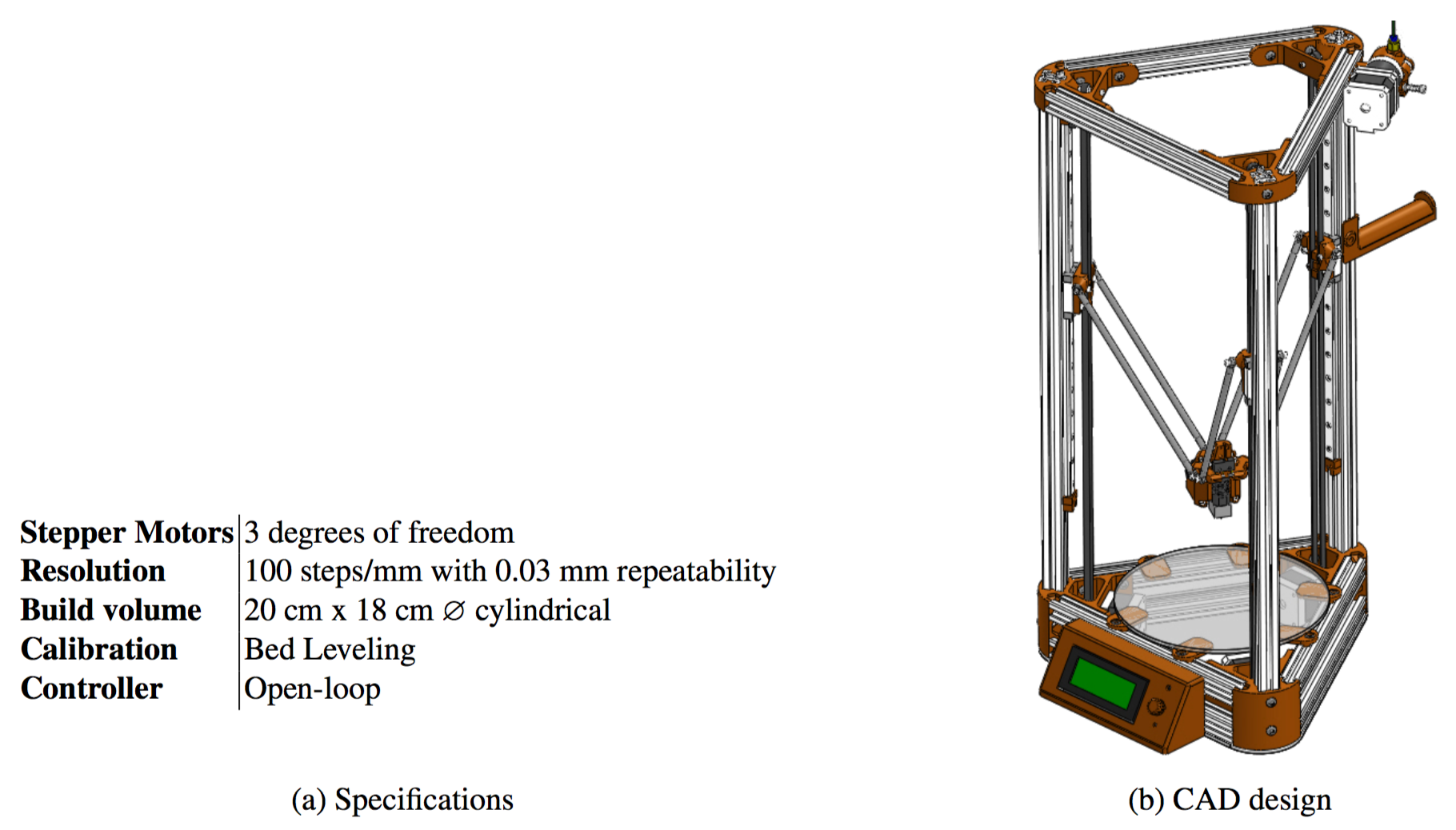
Similar to the camera, recent printer electronics allow a wireless connection over WiFi to schedule prints, adjusting settings or for visual inspection of the process with a webcam9.
The printer is controlled with G-Code, a human readable language to control CNC mills, lathes, 3D printers and laser cutters. Listing 8 shows a typical excerpt of a G-Code program. Every line correspondents to one instruction and consists of at least one tuple. The first tuple of every line describes the operation (move, stop, set settings). Following tuples are optional parameters whose meaning is depending on the operation. Every class of machine has their of dialect of G-Code. The RepRep community agreed on a dialect for 3D printers10.

5 Results
The following images are showing the intermediate steps of the processing pipeline which is described in Section 3. The results have been produces with the Pastie tool. It comes with a variety of more PCB images, scans and Gerber files which have been collected during this seminar.


6 Conclusion & Outlook
This work was focused on the development of a software tool for solder pad detection and printer control. Apart from that, the developed software can act as an universal front-end for OpenCV. This allows fast evaluation of new algorithms by interactively changing parameters by hand. In the future, this tool shall be extended to handle more complex tasks of the PCB assembly process.
The software can work with a variety of different data sources as photographies, scans and Gerber files. Even screenshots of the CAD tool or datasheets are usable. This is an advantage to existing methods, where layout data is required.
The quality of results is also depening on the surface finish of the PCB. Hot Air Solder Leveling (HASL) coats the solder pads with a thin film of tin. Unfortunatly, this results in an uneven surface finish which highly reflective. To cope with bright spots and reflexions a diffuse illumination is essential. Electroless Nickel Immersion Gold (ENIG) or Immersion Tin (ISn) coating in contrast, will result in a even and soft surface with a yellow / golden color.
Another influencing factor is the color of the silkscreen and solder resist. The solder resist is a thin mask which is applied to the bare PCB to protect the traces from oxid. Common colors for solder resists are green, black, white and blue. Best results were achieved with black to gain a high contrast.
There is still a lot space for further usability improvements. At the current state, pictures and G-Code instructions are transferred with memory cards between the camera, printer and PC. This can be simplified by using the existing WiFi capabilities of those devices. The import of Gerber files is currently only possible by using a conversion tool called gerbv. However, it provides a software library called libgerbv to facilitate the import of Gerber files as part of the implementation.
Within the scope of this seminar, a detailed evaluation of the results and testing was not possible due to the limited amount of time. It is eligible to compare the results the of camera based analysis with a Gerber based one of the same PCB. In doing so the deviation between the original CAD data and their reconstruction can be evaluated. For real application, a dispenser tool head for the printer is missing and has to be designed. It’s desirable to use the existing 3D printing technology to do this.
The results in this paper are showing, that existing standard algorithms are sufficient for the detection of solder pads. However there are situations in which they fail. In these cases a segmentation based on the Watershed algorithm or using the Harris corner detection may be used to improve the results.
7 Literature and Materials
- [BreierLfB] Rotation Estimation for Printed Circuit Board Recycling by Matthias Breier et. al. (LfB, 2014)
- [MVGeom] Multiple View Geometry in Computer Vision by Richard Hartley, Andrew Zisserman (Cambridge University Press, March 2004)
- [LearnOCv] Learning OpenCV by Gary Bradski und Adrian Kaehler (O’Reilly & Associates, October 2013)
- [OCvDoc] OpenCV Documentation and referenced papers: http://www.opencv.org/
- [QtDoc] Qt Project Documentation: http://www.qt-project.org/
- [RRap] RepRap Project Wiki: http://reprap.org/wiki/
7.1 Links and Software
- Pastie The implementation: https://github.com/stv0g/pastie/
- GerbV Gerber File Viewer and Library: http://gerbv.geda-project.org
- libqt-omd Communication library for Olympus OM-D & Pen cameras: https://github.com/stv0g/libqt-omd/
- Logitech HD Pro C920: 2304×1536 pixel with autofocus.
- libgerbv is a free software library for rendering Gerber files.
- See OpenCV function getPerspectiveTransform().
- The silkscreen contains printed markers and text on top of the PCB.
- See OpenCV function getAffineTransform().
- The solder paste extruder itself is not part of this work.
- libqt-omd is available as free software at http://github.com/stv0g/libqt-omd.
- Pastie is available as free software at https://github.com/stv0g/pastie.
- This functionality is provided by a software called Octoprint: http://www.octoprint.org.
- The dialect is documented on the RepRap website: http://reprap.org/wiki/G-code.